SiP System-in-Package
3D Plus
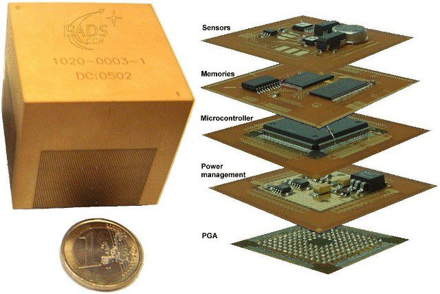
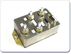
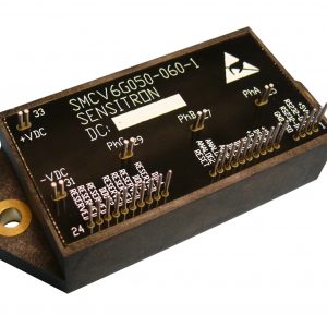
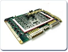
A System-In-Package (SiP) consists of a number of dissimilar integrated circuits enclosed in a single highly miniaturized package. The SiP performs all or most of the functions of an electronic system, and, it can contain several silicon components (bare die or package) and passive components.3D Plus provides a one-stop source for customer’s concept analysis, feasibility study, design, manufacturing and test of High Reliability and High Performance SiP.
Our State-of-the Art stacking technologies for SiP allow us to bring the best standard semiconductor devices and technologies in one single highly miniaturized package with almost no limit for the merging of heterogeneous technologies (Die – package – Passives).
Achieving a combination that cannot be realized with monolithic System-on-Chip (SoC) approaches, and, relying on a proven “first time right” design and development methodology, 3D Plus SiP stacks are more effective and have also a lower development cost and a faster time to market. More information
START YOUR SiP DESIGN HERE
Summarize the following information to submit your custom SiP concept analysis and feasibility study:
- Part list (final or preliminary)
- Block diagram (if available)
- Main electrical featues (voltages, currents, operating frequency, …)
- Power dissipated
- Module max size
- Module Mounting technology
- Module I/O number
- Other characteristics (environement specification, quantity, quality grade,…)
Key Features
- Very small form factor and low profile (more than 80% reductions in size and weight + up-system and in service induced benefits)
- Heterogeneous systems : ability to merge different die, package technologies (flip-chip, FBGA, SOT, SOP,….) and form factors
- Improved reliability : space qualified stacking technology, fewer connectors and solder-joints, rugged to extremely harsh environments
- Improved performance : improved speed and signal integrity (less parasitic elements)
- Improved flexibility : modular design enables low-cost system changes, reduce PWB application routing complexity
- Design secrecy : encapsulated 3D Stacks are hard to reverse-engineer
- Improved time-to-market : Ability to achieve greater functionality in a time-to-market window than silicon integration cannot meet
- Proven “first time right” design and development methodology
- Recognized turn-key design, manufacturing and test
- Flexible business model and supply chain management from multi-unit to mass manufacturing
Technic
- 3D Plus provides four different very flexible Stack Technology Flows that can be used for the design of various styles of SiPs:
- Standard Packages Stack
- Flex Process – Die Stack
- Flex Process – SiP Stack (Heterogeneous components and mixed technology stacks)
- Wafer Level Stack – WDoD™
- Depending on the SiP performance requirements and targeted market, the relevant stacking process will be selected within 3D Plus technology portfolio in order to bring the best added value and benefits for our customer designs.
Design Flow & Quality Assurance
- As highly integrated applications require a close partnership between the Customer and 3D Plus engineers to get the highest benefit from the 3-D Technology, the SiP design flow is organized as per our proven “first time right” design and development methodology.
Further to the Initial Concept Analysis and Feasibility Study that is part of the Request For Quotation Process (Activity performed free of charge by 3D Plus), It includes five majors steps and four Customer oriented milestones revues where: - the SiP electrical schematics and part list are provided by the customer,
- the SiP detailed feasibility study and design activities are performed by 3D Plus with close links with the users engineers,
- the electrical tests are conducted in partnership with the customer.
